 A professional manufacturer of UVLED curing systems
UVA and UVC Light Meters-UVEN300
745UV Light Meter
View detailsSearch the whole station
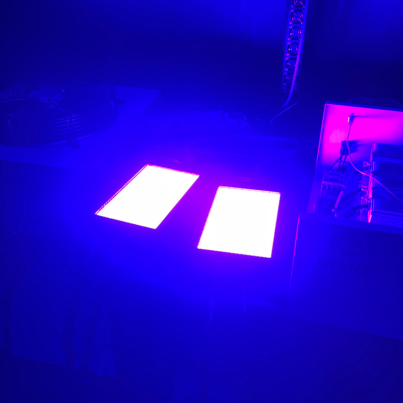
Photovoltaic silicon wafers are the core material of solar cells, and their production process requires the use of various chemicals and adhesives such as glue. Traditional curing methods require the use of UV lamps, which are not only bulky, but also have high energy consumption. In recent years, with the development of UVLED technology, more and more photovoltaic silicon wafer production enterprises began to use UVLED light curing technology, which has the advantages of low energy consumption, high efficiency, safety and environmental protection.
First,the basic principle of UVLED light curing technology.
UVLED light curing is a technology that uses UVLED to emit ultraviolet light to cure the adhesive. When the UV radiation to the adhesive surface, the monomer and low molecular weight substances in the adhesive will cross-link reaction, the formation of high molecular weight polymer, so that the adhesive becomes strong, durable. UVLED light curing technology has the following characteristics:
1, high efficiency: UVLED light efficiency is high, can complete the light curing process in a short period of time to improve production efficiency.
2, low energy consumption: UVLED light source can efficiently convert electrical energy into light energy, compared to traditional UV lamps lower energy consumption.
3, safe and environmentally friendly: UVLED light source without ultraviolet radiation and mercury pollution, harmless to the environment and the operator.
Second, UVLED light curing in the production of photovoltaic silicon wafer applications
UVLED light curing in the production of photovoltaic silicon wafers are mainly used in the following areas:
1, backplane curing
The backsheet is an important part of the photovoltaic cell, its main role is to protect the cell components and provide support. In the production process, the backsheet needs to be bonded to the cell and cured to make it tightly bonded. Traditional curing methods require the use of lamps, while UVLED light curing technology can achieve efficient, safe and stable curing effect.
2, silicon wafer bonding
UVLED light curing technology can achieve a more uniform and efficient curing effect, thus improving the quality and efficiency of the cell module.
3、Transfer film
In the manufacturing process of PV wafers, it is also necessary to use transfer film to make cell chips. Traditional curing methods require the use of ultraviolet lamps, while UVLED light curing technology can achieve a more efficient and safe curing effect, thereby improving the manufacturing efficiency and quality of battery components.
Third, the advantages of UVLED light curing technology
The use of UVLED light curing technology in the production process of photovoltaic silicon wafers has the following advantages:
1, energy saving and emission reduction
UVLED light source energy consumption is more than 50% lower than traditional UV lamps, while UVLED light source does not contain mercury and other harmful substances, can greatly reduce environmental pollution and harm.
2, improve production efficiency
UVLED light curing technology has a highly efficient, fast and uniform curing effect, can improve production efficiency and production quality.
3, reduce production costs
UVLED light source has a long life, low maintenance costs and other advantages, can reduce production costs.
Fourth, concluding remarks
The emergence of UVLED light curing technology has greatly contributed to the progress of photovoltaic wafer production technology, improving production efficiency and product quality, while also meeting environmental requirements. In the future, with the continuous development of UVLED technology, its application in the production of photovoltaic wafers will be more widespread.


UV curing adhesives emerge as an optimal solution for lens bonding owing to their rapid curing times and ability to forge strong, optically clear bonds. LED curing devices facilitate expedited assembly processes for manufacturers without compromis...
View details
UV LED curing technology is making a significant impact in the medical device industry.
View details
UVLED light sources are highly useful in the optical communication industry
View details